


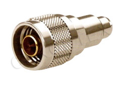
| Temperature range | -65~+125℃ | Insulation resistance | ≥5000MΩ | |
| Characteristic impedance | 50Ω | Dielectric withstanding voltage | 1000V | |
| Frequency range | 0~18GHz | Contact resistance | Center conductor | ≤0.003Ω |
| VSWR | ≤1.15+0.012f | Outer conductor | ≤0.002Ω | |
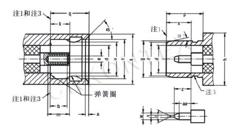
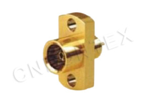
| Symbol | MIN (mm) | MAX (mm) | Note | Symbol | MIN (mm) | MAX (mm) | Note |
| a | 0.38 | 0.51 | Chamfer | q | 一 | 5.029 | |
| b | 2.845 | 一 | 4,6 | s | φ7.370 | 一 | |
| d | φ4.090 (Nominal value) | Diameter | t | φ5.720 | 一 | Diameter | |
| e | - | 二 | 2 Diameter | u | 一 | 一 | Diameter |
| f | φ4.880 (Nominal value) | Diameter | V | 一 | 0.380 | 4 Diameter | |
| g | 5.309 | 5.359 | Diameter | W | φ0.9017 | φ0.9398 | Diameter |
| h | φ7.620 (Nominal value) | Diameter | X | 3.252 | 3.429 | Diameter | |
| k | 3.048 | 3.225 | 3 | Z | 2.159 | 2.413 | |
| m | 2.921 | 一 | aa | 1.346 | 一 | ||
| p | 5.055 | 一 | - | - | 一 | 一 | |


Tel


Top
