QMA PCB Connectors: Mounting A Snap-On Interface On A Board
Release time:2026-11-09
Visits:27
The QMA coupling was invented to take a torque wrench out of the field. That trade — speed in exchange for an axial push — lands on the PCB designer's desk, because whatever force it takes to snap a plug on has to go somewhere. On a cable-to-cable QMA that force disappears into the cable assembly. On QMA PCB connectors it goes into two or four solder joints, the copper pad under them, and the laminate underneath that. Get that path wrong and the connector survives while the board does not.
The Mechanical Brief Comes First
Most RF connector selection starts with frequency. For a board-mounted snap-on part, it should start with force.
The Load Path Runs Through the Board
A threaded SMA spreads its mating load through the threads and into a coupling nut, so the board only sees what the nut transfers. A snap-on interface transfers the full insertion and withdrawal force axially through the body of the connector into its mounting feature. With a four-hole flange, that load goes into four screws and the panel or board around them. With a through-hole body, it goes into the solder fillets.
The practical consequence is that a
QMA flange connector on a 1.6 mm board behaves very differently from the same part on a 2.4 mm board with a stiffener. Thin laminate flexes under the snap, the fillet sees a peel load instead of a shear load, and a crack opens after a few hundred mating cycles rather than a few thousand.
Mating Force and Board Stiffness
Snap-on interfaces need a defined insertion force to seat and a defined retention force to stay seated. Both are specified by the coupling design, not by the board. What the board controls is how much of that force becomes bending. Two rules cover most cases: keep the connector within 15 mm of a mounting point or a stiffener, and never let a QMA flange overhang a board edge without a mechanical support behind it.
The Electrical Baseline You Inherit
QMA keeps the internal geometry of an SMA and changes only the coupling, so the electrical performance is close to what an SMA gives you on the same footprint. KONTEX publishes the following for the series.
|
Parameter |
Value |
|
Characteristic impedance |
50 Ω |
|
Frequency range |
DC – 18 GHz |
|
VSWR, DC – 3 GHz |
typically 1.052 |
|
Insertion loss |
< 0.06 √f(GHz) dB |
|
RF leakage |
down to −120 dB, DC – 3 GHz |
|
Power handling |
up to 75 W at 10 GHz, 25 °C |
|
Durability |
500+ mating cycles |
|
Body and plating |
brass, ternary alloy plating |
|
Dielectric |
PTFE |
Low PIM Is a Material and Plating Story
Passive intermodulation is generated where two metal surfaces touch imperfectly. In a snap-on connector the contact points are the outer spring fingers and the inner socket, and both are sensitive to plating quality, contact pressure and contamination. A
QMA connector that measures well on VSWR can still generate PIM if the plating is thin or the fingers have lost tension. For base station and distributed antenna work, ask for the low PIM variant explicitly and keep the mating surfaces clean and dry.
Mount Styles You Will Actually Use
The
KTX QMA range covers the mounting options that appear on real boards and panels. The choice between them is a mechanical decision with electrical consequences.
|
Mount style |
Typical KTX part |
Board implication |
|
Four-hole flange, solder pin |
QMA-KFD, QMA-KFD3, QMA-KFD5-3 |
Screw-fixed body; load bypasses the solder joint |
|
Cable connector, straight |
QMA-KHD9 |
No board interface; strain relief in the harness |
|
Right-angle cable version |
QMA-KYHD |
Lower profile, higher bending load at the boot |
|
Compact PCB body |
QMA-KYB2, QMA-KYB3 |
Small footprint, load carried by the solder joints |
Four-Hole Flange With a Solder Pin
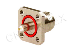
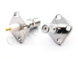
This is the safest arrangement on a thin board, and it is the one most often used in production. The flange takes the snap force through its screws, and the solder pin carries current only. The pin still needs a proper fillet, but it is no longer a structural element. Align the flange holes with the ground plane so the screws tie the body to the same reference as the launch.
Through-Hole Legs and Compact Bodies
Where space rules out a flange, a compact PCB body is the alternative, and the design has to compensate for the missing screws. That means more ground vias close to the body, a local copper pour on both layers, and a mechanical anchor such as a slot or a bracket if the connector will be mated in the field rather than once at build.
Footprint Rules That Save Debug Time
Ground Vias and Return Current
At 10 GHz the return current does not spread across the plane — it follows the launch. Put ground vias within one dielectric thickness of the connector body, on both sides of the launch, and connect them to the ground plane the signal reference actually uses. A launch with a beautiful signal pad and two distant ground vias will show a resonance long before 18 GHz.
Keep-Out and Coplanarity
The keep-out is not just for the body. It has to cover the sweep of the coupling nut and the fingers of the mating plug, plus the finger space needed to release the snap. A connector that needs a tool or a screwdriver to demate on a crowded board is a field failure waiting for a service visit. For flange parts, check coplanarity of the four mounting feet against the board surface; a 0.1 mm gap becomes a bent flange when the screws are torqued.
Soldering a Snap-On Interface
Reflow Versus Iron
A flange connector with a single solder pin reflows cleanly and gives a repeatable fillet. A multi-leg PCB body is better reflowed with the rest of the board, using a stencil aperture that leaves enough solder for a concave fillet without wicking into the interface. Hand soldering works for prototypes and repairs, but the iron tip must not touch the dielectric: PTFE softens and the centre pin shifts, which shows up later as a VSWR bump at the top of the band.
Cleaning and Sealing
Flux residue inside the interface is a slow-acting failure. Clean before mating, cap the connector during board wash, and use a sealing boot on any outdoor or washdown assembly. Snap-on interfaces are more tolerant of slight misalignment than threads and less tolerant of grit.
Verification Before Release
A short checklist catches nearly every board-level QMA problem before tooling is cut.
|
Check |
Target |
Why it matters |
|
Mating force measured on a first article |
within the coupling specification |
High force signals a tight or damaged body |
|
Pull test after 50 mates |
no fillet cracking, no pad lift |
Proves the load path, not just the solder joint |
|
VSWR sweep to 18 GHz |
flat, no resonance below 12 GHz |
Catches launch and ground via mistakes |
|
Ground via count and spacing |
within one dielectric thickness |
Controls return current at the launch |
|
Keep-out versus mating plug envelope |
full sweep plus finger access |
Avoids unserviceable assemblies |
A Practical Summary
QMA PCB connectors are a good answer when a board has to be connected and reconnected often, in a place where a wrench does not fit. They are a poor answer when the board is thin, unsupported, and expected to take the snap force through two solder joints. Decide the mount style on mechanical grounds first — flange where the load must bypass the laminate, compact body only where the board is stiff and the mating count is low — and the electrical design becomes a normal 18 GHz launch exercise.
KONTEX builds the QMA range, including flange and PCB versions, in Zhenjiang, Jiangsu, and publishes the electrical and mechanical data needed to close a design review without a round of emails.